Ok as promised, here's a very simplified guide to how organic chemistry works. As mentioned before, the basis to all chemistry is understanding how electrons interact. I'll assume everyone reading will have at least GCSE science (ie upto age 16 for non-UK types).
Classical physics believed that microscopic system behave in the same way as macroscopic systems, but this wasn't the case. At the start of the 20th century the idea of quantum physics was born. The upshot of this was the discovery atoms and molecules have certain discrete energy levels and electrons must sit in one of these - they cannot sit between levels. Electrons always prefer to sit in the lowest energy state possible (called the ground state), but can be temporarily "excited" to a higher level if energy is put into the system. Once the energy is removed, the electron will relax back down to the ground state.
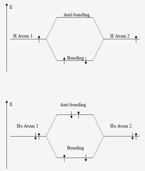
Electrons orbit the nucleus of an atom in orbitals. When 2 or more atoms approach each other, the orbitals can overlap and bonds can form. There are 2 types of overlap -
in phase and
out of phase.
In phase overlaps lead to a situation where the combined energy of the overlap is less than that of the individual atoms. The resultant orbital is called a
bonding orbital.
Out of phase overlaps lead to a higher energy than that of the individual atoms. These are
anti-bonding orbitals. All of the electrons from the individual atoms must be fitted into the new
molecular orbitals, those that won't fit in the bonding orbital must go into the antibonding orbital. Overall, the
bond order of the new molecule is calculated as being (number of bonding electrons - number of anti-bonding electrons)/2. In the example below, the 2 atoms are hydrogen and the resultant molecule is H
2 with a bond order of 1. If the 2 atoms were helium, then the molecular orbitals would have 2e in the bonding and 2e in the anti-bonding orbitals giving a bond order of 0. This indicates that the molecule He
2 does not form.
If you're interested in learning more about how chemical bonds form, I can recommend the OCP primer
Chemical Bonding by Mark Winter. It's a very short book that's not overly technical and it's only about
£3.50 second hand from Amazon.
Because orbitals closer to the nucleus have lower energy, in complex, multi-electron molecules, most of the molecular orbitals can be ignored for our purposes. For OLEDs (and much of organic chemistry), we are only interested in the highest molecular orbital that contains electrons (the
HOMO) and the next molecular orbital above that (with no electrons - the
LUMO).
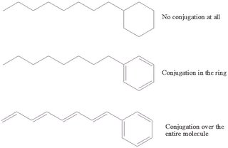
The last important feature that needs to be touched upon is that of
conjugation. If the bond order for a diatomic molecule is 2 then it has a double bond. In the case that you get alternating single and double bonds in a polyatomic molecule then the electrons can freely wander around this entire area. This is energetically favoured and lowers the energy levels. The electrons are said to be
delocalised as they are not necessarily in the double bond as drawn. In this way any charge that is induced in these types of molecule can be transported down the length of the conjugated parts of the molecules.
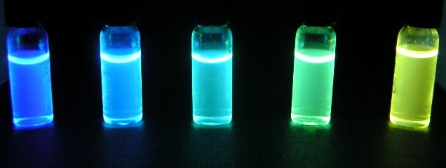
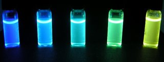
As mentioned above, when energy is put into the molecule (eg by irradiating with UV light), an electron can jump from from the HOMO to the LUMO. As is when it relaxes back to the ground state, the energy released can be given out as light. The difference in energy between the HOMO and LUMO determines the wavelength of the emitted light. Sometimes that wavelength falls in the range of human vision (~380 - 750nm) and we perceived light. When light is used to excite molecules in this way it is called
photoluminescence (PL). Another way to produce this effect is to put a potential difference (ie voltage) across the molecules - this is known as
electroluminescence (EL) and this forms the basis of OLED emission. Below is an example of some solutions displaying PL (excited by long wavelength UV light).
The mechanism of emission works as follows. As a potential is applied, the cathode injects electrons into the LUMO of the material (as no further electrons will fit into the HOMO of the materials we use) producing a negatively charged
polaron. At the same time the anode removes electrons from the HOMO of material (termed an
injection of holes due to the fact that a "hole" has been introduced in the HOMO) producing a positively charged polaron. Under the influence of the electric field, these charges move towards the electrode of opposite charge, bytravelingg down conjugated sections of molecules and by "hopping" from one molecule to another. If they encounter each other on the way then they can combine to produce an excited state molecule like those seen in photoluminescence. Once the electrons in the LUMO relax back down to the ground state and can emit light.

So far so simple. However, for everything to work well a number of criteria need to be met. The electrodes have energy levels (
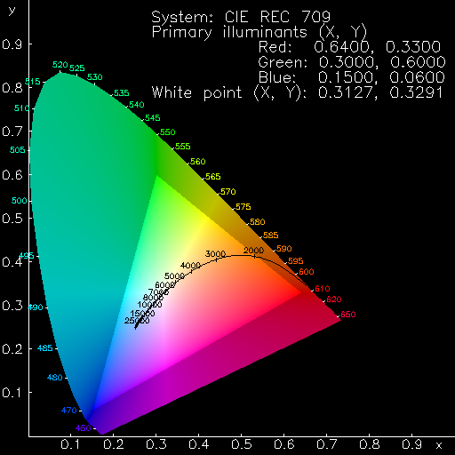
work functinons - the amount of energy required to remove an electron).In order to be as efficient as possible, the energy level of the cathode must match that of the LUMO of the emissive material, and the energy level of the anode must match that of the HOMO - the further away from this ideal, the more potential has to be applied to "force" electrons and holes into the material - high potentials can cause damage to the molecules and cause the device to fail. Once inside the material, both sets of polarons should be conducted at equal rates, but unfortunately due to the nature of most materials transport of one polaron is usually favoured over the other. This can lead to the polarons simply reaching the opposing electrode and being quenched - therefore emitting no light. Of course, the emissive material must also possess a HOMO-LUMO gap of the correct size to ensure that the light emitted is of the desired colour. Small gaps lead to red emission and large gaps lead to blue emission. The diagram on the left is known as a CIE diagram and displays colours as a function of wavelength. Through the middle is a line representing white light at different colour temperatures (similar to the effect of altering the white balance on a digital camera).
A good workaround to some of these problems is to introduce transport/blocking materials. The example below shows the use of a electron conducting/hole blocking layer - because it has a LUMO closer to the energy of the cathode, it more readily accepts the injection of electrons and due to the low-lying HOMO, the passage of holes towards the cathode is blocked. These extra materials can be added in several ways - by forming a physically distinct layer between the emissive layer and the cathode or by being mixed with the emissive layer. If the specific properties that define the material's good electron transport of hole blocking ability are known, then these features can be chemically built into the emissive layer itself. All 3 methods have draw backs - adding new layers makes fabrication of devices harder, blended layers can separate out over time and of course, altering the makeup of the emissive material will change it's HOMO-LUMO gap.
You can probably now see the challenge facing chemists - not only do their molecular designs have to allow for balancing charge transport and colour of emission, but they then have to actually make the thing which is often the hardest part.
The story doesn't end there -theree are many more materials that need to be considered for the anode (at the moment indium-tin-oxide (ITO) is used as it is transparent and allows the light generated to leave the device), cathode, substrate and any encapsulents. The end result will be cheap, low power, bright, thin screens. Several prototypes like the one below are appearing at trade shows at the moment.

For another (probably better) explanation of OLEDs, have a look
here.
This blog will give you an insight into my work and any interesting developments from the field worldwide.